October 27, 2026
From Electronics to Photonics: The Next Era of AI Infrastructure (Part 2)
Type
Deep DivesSara Shabani
Sara Shabani
By Sara Shabani, Senior Associate at Cota Capital
Inside the Photonics Technology Stack and Value Creation
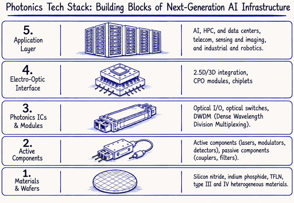
The photonics ecosystem spans a broad technology stack, with innovation at every layer. It begins with materials and wafers, such as thin-film lithium niobate (TFLN) and III–V heterogeneous materials, and extends through components such as lasers and modulators. Above these sit photonic integrated circuits and modules, including optical I/O and dense wavelength division multiplexing (DWDM), followed by the electro-optic interfaces that bring electronics and photonics together through co-packaged optics (CPO) and chiplet architectures. At the top are the application systems this technology serves, from AI and data centers to telecommunications and sensing. Each layer addresses a distinct engineering challenge, but together they form the foundation of next-generation AI infrastructure.
- Next-generation materials. New material platforms, particularly TFLN and heterogeneous III–V integration, enable modulators with higher bandwidth, lower optical loss, lower drive voltages, and greater energy efficiency than previous generations. They extend performance beyond silicon photonics while preserving the benefits of large-scale integration. The remaining challenge is manufacturing them at high yield and integrating them into complementary metal-oxide-semiconductor (CMOS)-compatible production flows at scale.
- Photonics ICs and modules. As AI clusters scale up into larger accelerator domains and out into more distributed deployments, photonic integrated circuits and optical modules are evolving from transceivers into programmable communication engines. Optical I/O, optical switching, and DWDM increase bandwidth density while reducing latency and energy per transmitted bit across chips, packages, racks, and eventually disaggregated memory pools. The next challenge is developing standardized, software-defined optical fabrics that can be deployed, monitored, and serviced at hyperscale.
- Electro-optic interfaces and advanced packaging. The interface between electronics and photonics is becoming one of the most strategically important layers of the stack. 2.5D/3D integration, co-packaged optics, and chiplet architectures bring optical and electronic functions closer together, shortening electrical path lengths while improving bandwidth, latency, and energy efficiency. As optics moves inside the package, differentiation shifts from device performance to packaging, assembly, testing, and yield, making advanced integration a key determinant of commercial success.
The Roadmap to the Optical AI Datacenter and Remaining Challenges
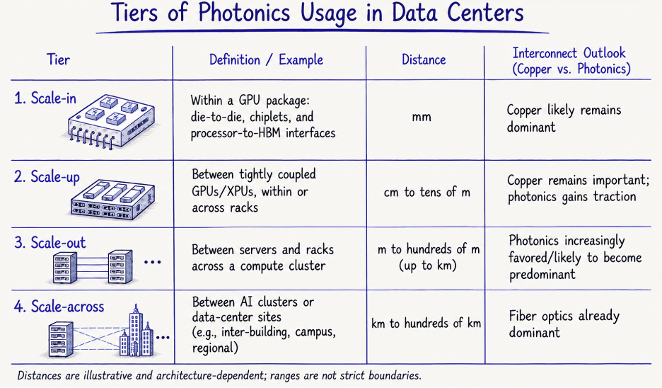
The move to photonics will not happen evenly across the data center, and it does not mean copper goes away. Even on a 10-year view, electrical interconnects are likely to remain important over the shortest distances. Based on current technology and industry roadmaps, photonics appears likely to move progressively closer to the GPU as bandwidth demands climb and the economics of moving data over copper become challenging.
Inside the GPU package, at the scale-in level, copper is likely to remain dominant. Across the millimeter-scale links between dies, chiplets, and high-bandwidth memory (HBM) electrical connections continue to win on the strength of very short paths and mature packaging.
Between GPUs in a rack, at the scale-up level, the boundary begins to blur. Copper still has a role, but photonics grows more attractive as accelerator fabrics scale and bandwidth density rises. Optical I/O and co-packaged optics help by moving electro-optic conversion closer to the processor, shortening the remaining electrical path.
Between servers, at scale-out, photonics may increasingly become the default. Over these distances, copper runs into real power and signal-integrity limits, and both performance and cost favor optics.
The same holds between cabinets and across wider data-center domains: at scale-across, optics is generally favored for the same reasons. The overall shift is less about photonics replacing copper than about the boundary between them moving inward.
The challenges that remain are more about commercialization than about scientific feasibility, and they cluster into three.
1. Thermal design and manufacturing yield. As optics moves into the package, co-packaged systems have to manage heat and hold high yield in high-volume assembly – two problems that get harder the closer the optics sit to the compute die. Testing and validation at scale remain just as demanding.
2. Economics across the hierarchy. The technology needs to be cost-effective across several layers of the data center at once – chip, package, rack, and cluster – rather than winning at one level and losing at another. Cost and yield ultimately determine whether any of these reaches commercial deployment.
3. Control and software. Optical switching brings its own control plane, telemetry, and contention management problems, and reconfigurable fabrics require better software abstractions for workload- and topology-aware orchestration. Without that software layer, an optical fabric ends up merely installed rather than exploited.
What Does This Mean for the AI Infrastructure Ecosystem?
For hyperscalers and AI data-center operators, the advantage shifts from accumulating compute to co-designing compute, memory, networking, and photonics as one system. Some of the most consequential decisions are architectural, not component-level: where to perform optical conversion, how large to make scale-up domains, and how to expose topology reconfiguration to schedulers and training frameworks. Operators increasingly appear to benefit from treating these as system-level questions rather than solely as procurement choices.
For researchers, the frontier is interdisciplinary, and breakthroughs will come from working across systems: device physics to packaging, packaging to architecture, and architecture to software. The latter – designing programmable network architectures and integrated photonics hardware together – is where recent roadmaps are converging.
For investors, the opportunity extends well beyond photonic components across several layers of the ecosystem. In electro-optic interfaces and advanced packaging, moving optics inside the package may increase the importance of assembly, alignment, and yield. In next-generation materials, platforms such as TFLN may benefit from an early manufacturing lead that compounds over time. And in photonic ICs and modules, optical networking – including I/O, switching, and the software and control layer above them – may become increasingly important as orchestration and interoperability requirements develop.
Share Story